- 您现在的位置:买卖IC网 > Sheet目录1242 > SFPA32GBQ1BO8TO-I-QT-223-STD (Swissbit NA Inc)FLASH SSD SMART UDMA 2.5" 32GB
�� �
�
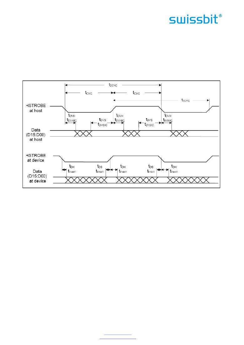
�a)� The� host� shall� drive� a� data� word� onto� D[15:00].�
�b)� The� host� shall� generate� an� HSTROBE� edge� to� latch� the� new� word� no� sooner� than� t� DVS� after� changing�
�the� state� of� D[15:00].� The� host� shall� generate� an� HSTROBE� edge� no� more� frequently� than� t� CYC� for� the�
�selected� Ultra� DMA� mode.� The� host� shall� not� generate� two� rising� or� falling� HSTROBE� edges� more�
�c)�
�frequently� than� 2t� cyc� for� the� selected� Ultra� DMA� mode.�
�The� host� shall� not� change� the� state� of� D[15:00]� until� at� least� t� DVH� after� generating� an� HSTROBE� edge�
�to� latch� the� data.�
�d)� The� host� shall� repeat� steps� (a),� (b),� and� (c)� until� the� data� transfer� is� complete� or� an� Ultra� DMA� burst�
�is� paused,� whichever� occurs� first.�
�Figure� 9:� Sustained� Ultra� DMA� Data-Out� Burst� Timing�
�Note:� Data� (D15:D00)� and� HSTROBE� signals� are� shown� at� both� the� device� and� the� host� to� emphasize� that�
�cable� settling� time� as� well� as� cable� propagation� delay� shall� not� allow� the� data� signals� to� be� considered�
�stable� at� the� device� until� some� time� after� they� are� driven� by� the� host.�
�6.3.2.4.8� Device� Pausing� an� Ultra� DMA� Data-Out� Burst�
�The� device� pauses� an� Ultra� DMA� Data-Out� burst� by� following� the� steps� lettered� below.� The�
�timing� diagram� is� shown� in� Figure� 10:� Ultra� DMA� Data-Out� Burst� Device� Pause� Timing.� The�
�timing� parameters� are� specified� in� Table� 22:� Ultra� DMA� Data� Burst� Timing� Requirements� and� are�
��The� following� steps� shall� occur� in� the� order� they� are� listed� unless� otherwise� specifically� allowed:�
�a)� The� device� shall� not� pause� an� Ultra� DMA� burst� until� at� least� one� data� word� of� an� Ultra� DMA� burst� has�
�been� transferred.�
�b)� The� device� shall� pause� an� Ultra� DMA� burst� by� negating� -DDMARDY.�
�c)� The� host� shall� stop� generating� HSTROBE� edges� within� t� RFS� of� the� device� negating� -DDMARDY.�
�d)� If� the� device� negates� -DDMARDY� within� t� SR� after� the� host� has� generated� an� HSTROBE� edge,� then� the�
�device� shall� be� prepared� to� receive� zero� or� one� additional� data� words.� If� the� device� negates� -�
�DDMARDY� greater� than� t� SR� after� the� host� has� generated� an� HSTROBE� edge,� then� the� device� shall� be�
�prepared� to� receive� zero,� one� or� two� additional� data� words.� The� additional� data� words� are� a� result�
�of� cable� round� trip� delay� and� t� RFS� timing� for� the� host.�
�e)� The� device� shall� resume� an� Ultra� DMA� burst� by� asserting� -DDMARDY.�
�Swissbit� AG�
�Industriestrasse� 4�
�Swissbit� reserves� the� right� to� change� products� or� specifications� without� notice.�
�Revision:� 1.00�
�CH-9552� Bronschhofen�
�Switzerland�
�www.swissbit.com�
�industrial@swissbit.com�
�P-120_data_sheet_PA-QxBO_Rev100.doc�
�Page� 26� of� 76�
�发布紧急采购,3分钟左右您将得到回复。
相关PDF资料
SFPK-SL
CONN SFP CAGE
SFSA16GBV1BR4TO-I-QT-226-STD
FLASH SLC UDMA/MDMA/PIO 16GB
SFSA32GBQ1BR8TO-I-QT-226-STD
FLASH SLC UDMA/MDMA/PIO 32GB
SFSA32GBU1BR4TO-I-NC-216-STD
FLASH X-200M SLC MSATA 32GB
SFSA32GBV1BR4TO-I-NC-216-STD
FLASH X-200S SLC SLIM SATA 32GB
SFSA64GBQ1BR8TO-I-NC-216-STD
FLASH SSD UDMA IND 2.5" 64GB
SFSO4404NR
FEMALE SCREWLOCK 4-40 .197"
SFW22R-1STE1
SFW22R-1STE1-FFC/FPC CONN
相关代理商/技术参数
SFPA32GBQ1BO8TO-I-QT-243-STD
制造商:SWISSBIT NA INC 功能描述:FLASH
SFPA36AT0250
制造商:General Electric Company 功能描述:SFP 3P 600V 250A
SFPA4096Q1BO2TO-C-DT-243-STD
制造商:SWISSBIT NA INC 功能描述:FLASH
SFPA4096Q1BO2TO-I-DT-223-STD
功能描述:FLASH SSD SMART UDMA 2.5" 4GB RoHS:是 类别:计算机,办公室 - 元件,配件 >> 固态硬盘驱动器 系列:P-120 标准包装:1 系列:- 存储容量:64GB 存储器类型:闪存 - NAND 其它名称:VL 64 GB SSHD KITVL64GBSSHDKIT
SFPA4096Q1BO2TO-I-DT-243-STD
制造商:SWISSBIT NA INC 功能描述:FLASH
SFPA-53
制造商:未知厂家 制造商全称:未知厂家 功能描述:Schottky Barrier Diodes
SFPA-63
制造商:SANKEN 制造商全称:Sanken electric 功能描述:Schottky Barrier Diodes (Surface Mount) 30V
SFPA-73
制造商:未知厂家 制造商全称:未知厂家 功能描述:Schottky Barrier Diodes